MX3 AI Accelerator Datasheet#
1. Introduction#
This datasheet provides a technical description of the MemryX MX3 Edge AI accelerator.This document should be read in conjunction with other board and hardware integration guides for designing in a PCB/motherboard.
The MX3 AI Accelerator is designed to be connected directly to a system host processor using a PCIe or USB interface. It is designed to offload AI processing from the host, where the host can be one of many popular x86, Arm, or RISC-V based processors. OS support includes Windows and multiple Linux distributions.
The MX3 is designed with a dataflow architecture, making it most efficient when used in pipelined operation (e.g., continuously streaming inputs such as cameras). Host inputs are streamed directly into the Compute Engines on one or more MX3 Accelerators (MXA), where AI processing occurs, and output is returned to the host.
Key Features:#
Total Weight memory: 10.5MB
Total Feature map memory: 5MB (custom format, do not use for calculating model support)
External/Host Interfaces: PCIe Gen 3 2-lanes (8Gbps x2) or USB3 Gen 1 x1 (5Gbps x1)
Chip-to-Chip Interface: PCIe Gen 3 2-lanes (8Gbps x2)
Any frequency between 200MHz and 1000MHz in 25MHz steps.
Corresponding voltages between 0.68V and 0.85V in 5 mV steps.
Typical Power used is approximately 0.5W - 3W per chip (depending on system configuration and AI workload)
Multiple MX3 chips can be used together as one logic unit, supporting up to 16 chips on a board using a single interface to the host.
9x9mm FC-FBGA
2. Overview#
The MX3’s architecture is tightly integrated with MemryX’s SDK, ensuring maximum hardware efficiency and AI model performance (inference rate, accuracy, latency). At the heart of MX3 lies the custom-designed MemryX Neural Processing Unit (NPU), an AI accelerator designed with MemryX’s patented scalable at-memory dataflow architecture optimized for a wide range of vision-based AI inference models. Each accelerator is typically used as shown in Figure 1.
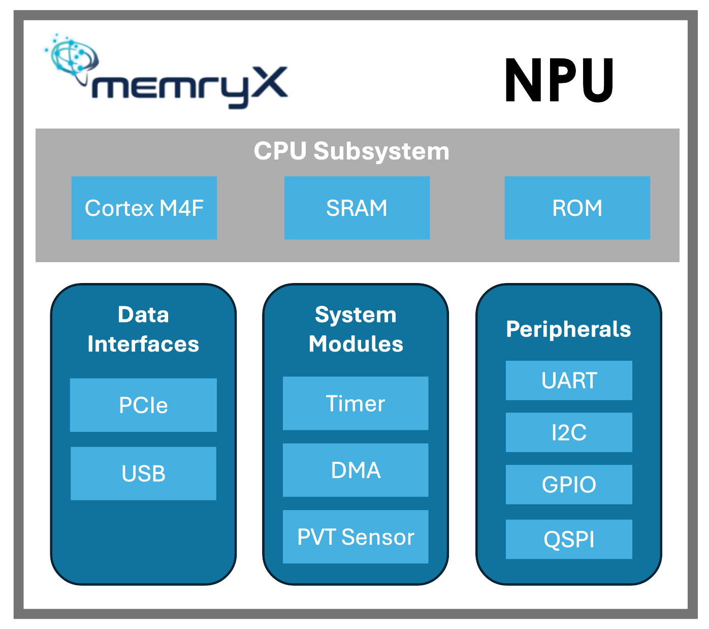
Figure 1 - MX3 Block Diagram#
2.1 NPU#
MemryX NPU Specifications:
Performance: Up to 6 TFLOPS per chip (1GHz)
Activation data format: Group-BF16
Weight data format: INT8 / INT4, INT16 via software
Parameter storage: Up to 10.5M (INT8) or 21M (INT4) AI model parameters
Supported Operators: Visit MemryX’s online Developer Hub for an up-to-date list of supported operators.
2.2 Data Interfaces#
PCIe Gen 3 x2: For host connectivity and inter-MX3 connectivity:
Dual-role controller that can function as a root port or an endpoint
One or two lanes (8GT/s per lane) are used for host connectivity on the first chip in a multi-chip configuration
Subsequent chips can use one or two lanes for chip-chip connectivity
USB 3.1 Gen 1: For host connectivity:
USB 3 device with USB 2 backward compatibility
Data rate: 5Gbps (Super-speed mode) / 480Mbps (High-speed mode)
2.3 Peripherals#
MX3 provides the following common industry-standard peripherals for debugging and low-speed communication.
Two UARTs: For logging and debugging
One I2C: For controlling and reading other components, such as power management ICs and temperature sensors
Up to 16 General Purpose I/Os (GPIOs): For status indication, error notification, etc.
QSPI: One QSPI master and one QSPI slave for booting from Flash
QSPI master supports booting from Flash as one of the boot modes
QSPI slave can be used to relay the boot image to another MX3 in multi-MX3 use cases
2.4 Other System Modules#
Two general-purpose timers: For time-keeping, performance monitoring, etc.
One watchdog timer: For SoC responsiveness monitoring
One General-purpose DMA: For data movement both inside MX3 and across data interfaces * Two DMA masters supporting up to 8 channels for parallel data movement
Sensors: Process, Voltage, and Temperature (PVT)
3. I/O Definitions#
3.1 Package Ball Map#
The MX3 is packaged in a 9x9mm FC-FBGA with 169 leads, with a ball size of 0.80 mm and a pitch of 0.65 mm. Figure 2 illustrates the ball map, highlighting power (pink) and ground balls (gray) , reference clock inputs (yellow), and high-speed signals (blue).
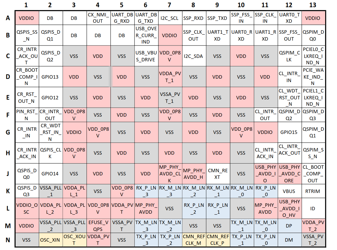
Figure 2 - MX3 Package Ball Map#
3.2 Pin Definitions#
The following table lists the pin definitions of the MX3 chip. The first column shows the ball number as defined in Figure 2. The second and third column lists the name and description of the pin. The fourth column shows the direction of the pin, which can be input (I), output (O), or bi-directional (I/O). And the last column lists if the chip has an internal pull-up/down resistor for the pin.
Table 1 - Pin Definitions
Ball Number |
Pin Name |
Description |
Direction |
Internal Pull Up/Down |
|---|---|---|---|---|
N2 |
OSC_XIN |
Primary clock source, 25MHz crystal XIN |
I |
|
N3 |
OSC_XOUT |
Primary clock source, 25MHz crystal XOUT |
O |
|
F1 |
PIN_RST_N |
External reset pin (active-low) |
I |
PU |
Ball Number |
Pin Name |
Description |
Direction |
Internal Pull Up/Down |
|---|---|---|---|---|
G2 |
CR_WDT_RST_IN_N |
Warm reset indication from chip on right |
I |
PU |
E12 |
CL_WDT_RST_OUT_N |
Warm reset indication to chip on left |
O |
PU |
E1 |
CR_RST_OUT_N |
Cold reset indication to chip on right |
O |
PU |
D1 |
CR_BOOT_COMP_IN |
Boot completion indication from chip on right |
I |
PD |
J13 |
CL_BOOT_COMP_OUT |
Boot completion indication to chip on left |
O |
PD |
G1 |
CR_INTR_IN |
Cascade chip on right interrupt in |
I |
PD |
C1 |
CR_INTR_ACK_OUT |
Cascade chip on right interrupt in acknowledgement |
O |
PD |
F2 |
CR_INTR_OUT |
Cascade chip on right interrupt out |
O |
PD |
H1 |
CR_INTR_ACK_IN |
Cascade chip on right interrupt out acknowledgement |
I |
PD |
D12 |
CL_INTR_IN |
Cascade chip on left interrupt in |
I |
PD |
H12 |
CL_INTR_ACK_OUT |
Cascade chip on left interrupt in acknowledgement |
O |
PD |
F11 |
CL_INTR_OUT |
Cascade chip on left interrupt out |
O |
PD |
H11 |
CL_INTR_ACK_IN |
Cascade chip on left interrupt out acknowledgement |
I |
PD |
A4 |
CX_NMI_OUT |
Cascade non maskable interrupt out |
O |
PD |
Ball Number |
Pin Name |
Description |
Direction |
Internal Pull Up/Down |
|---|---|---|---|---|
N8 |
CMN_REFCLK_M |
100MHz Reference clock differential Pair (-) |
I/O |
|
N9 |
CMN_REFCLK_P |
100MHz Reference clock differential Pair (+) |
I/O |
|
N11 |
TX_P_LN_0 |
High speed transmit data differential pair (+) |
O |
|
N10 |
TX_P_LN_1 |
High speed transmit data differential pair (+) |
O |
|
N7 |
TX_P_LN_2 |
High speed transmit data differential pair (+) |
O |
|
N6 |
TX_P_LN_3 |
High speed transmit data differential pair (+) |
O |
|
M11 |
TX_M_LN_0 |
High speed transmit data differential pair (-) |
O |
|
M10 |
TX_M_LN_1 |
High speed transmit data differential pair (-) |
O |
|
M7 |
TX_M_LN_2 |
High speed transmit data differential pair (-) |
O |
|
M6 |
TX_M_LN_3 |
High speed transmit data differential pair (-) |
O |
|
K11 |
RX_P_LN_0 |
High speed receive data differential pair (+) |
I |
|
L9 |
RX_P_LN_1 |
High speed receive data differential pair (+) |
I |
|
L8 |
RX_P_LN_2 |
High speed receive data differential pair (+) |
I |
|
K6 |
RX_P_LN_3 |
High speed receive data differential pair (+) |
I |
|
K10 |
RX_M_LN_0 |
High speed receive data differential pair (-) |
I |
|
K9 |
RX_M_LN_1 |
High speed receive data differential pair (-) |
I |
|
K8 |
RX_M_LN_2 |
High speed receive data differential pair (-) |
I |
|
K7 |
RX_M_LN_3 |
High speed receive data differential pair (-) |
I |
Ball Number |
Pin Name |
Description |
Direction |
Internal Pull Up/Down |
|---|---|---|---|---|
C13 |
PCIEL0_CLKREQ_IND_N |
PCIE clock request indication - L0. The L0 PM Substates use this signal to control the clocks |
I/O |
PU |
E13 |
PCIEL1_CLKREQ_IND_N |
PCIE clock request indication - L1. The L1 PM Substates use this signal to control the clocks |
I/O |
PU |
D13 |
PCIE_WAKE_IND_N |
PCIE wake indication |
I/O |
PU |
Ball Number |
Pin Name |
Description |
Direction |
Internal Pull Up/Down |
|---|---|---|---|---|
C6 |
USB_VBUS_DRIVE |
VBUS drive indication. Drive Vbus according to selected role and OTG protocol. When high VBUS should be driven by this device. |
I/O |
PD |
B6 |
USB_OVER_CURR_IND |
USB Overcurrent indication. Indicates that a given USB port has exceeded the maximum current allotted for that port. |
I/O |
PD |
M12 |
DP |
Full speed transmit differential pair (+) |
I/O |
|
N12 |
DM |
Full speed transmit differential pair (-) |
I/O |
|
L13 |
ID |
ID pin for USB receptacle |
I/O |
|
K12 |
VBUS |
VBUS Indication. Indicates when a host device has been connected to or disconnected from the USB peripheral. |
I/O |
Ball Number |
Pin Name |
Description |
Direction |
Internal Pull Up/Down |
|---|---|---|---|---|
A5 |
UART_DBG_RXD |
UART (debug) transmit data. Line used to transmit serial data. |
I |
PU |
A6 |
UART_DBG_TXD |
UART (debug) receive data. Line used to receive serial data. |
O |
PU |
A12 |
UART0_TXD |
UART 0 transmit data. Line used to transmit serial data. |
O |
PU |
B10 |
UART0_RXD |
UART 0 receive data. Line used to receive serial data. |
I |
PU |
B9 |
UART1_TXD |
UART 1 transmit data. Line used to transmit serial data. |
O |
PU |
B11 |
UART1_RXD |
UART 1 receive data. Line used to receive serial data. |
I |
PU |
Ball Number |
Pin Name |
Description |
Direction |
Internal Pull Up/Down |
|---|---|---|---|---|
C12 |
QSPIM_CLK |
Quad SPI master clock. Output clock to which the output serial data will be synchronized. |
O |
PD |
H13 |
QSPIM_SS_N |
Quad SPI slave select. Signal through this pin will be used to select the slave device. |
O |
PU |
B13 |
QSPIM_DQ0 |
Quad SPI data 0 (bi-directional). Data transmitted between the master and the slave. Line 0 of the four serial lines available (0-3) |
I/O |
PD |
G13 |
QSPIM_DQ1 |
Quad SPI data 1 (bi-directional). Data transmitted between the master and the slave. Line 1 of the four serial lines available (0-3) |
I/O |
PD |
F12 |
QSPIM_DQ2 |
Quad SPI data 2 (bi-directional). Data transmitted between the master and the slave. Line 2 of the four serial lines available (0-3) |
I/O |
PD |
F13 |
QSPIM_DQ3 |
Quad SPI data 3 (bi-directional). Data transmitted between the master and the slave. Line 3 of the four serial lines available (0-3) |
I/O |
PD |
H2 |
QSPIS_CLK |
Quad SPI slave clock. Input clock to which the input serial data will be synchronized. |
I |
PD |
B1 |
QSPIS_SS_N |
Quad SPI slave select. Signal through this pin will be used to select the current slave by an external QSPI master. |
I |
PU |
J1 |
QSPIS_DQ0 |
Quad SPI data 0 (bi-directional). Data transmitted between the master and the slave. Line 0 of the four serial lines available (0-3). |
I/O |
PD |
B2 |
QSPIS_DQ1 |
Quad SPI data 1 (bi-directional). Data transmitted between the master and the slave. Line 1 of the four serial lines available (0-3). |
I/O |
PD |
C2 |
QSPIS_DQ2 |
Quad SPI data 2 (bi-directional). Data transmitted between the master and the slave. Line 2 of the four serial lines available (0-3). |
I/O |
PD |
K1 |
QSPIS_DQ3 |
Quad SPI data 3 (bi-directional). Data transmitted between the master and the slave. Line 3 of the four serial lines available (0-3). |
I/O |
PD |
Ball Number |
Pin Name |
Description |
Direction |
Internal Pull Up/Down |
|---|---|---|---|---|
A11 |
SSP_CLK_IN |
SSP Serial Clock input. |
I |
PD |
B8 |
SSP_CLK_OUT |
Serial Clock Output pin. |
O |
PD |
A10 |
SSP_FSS_IN |
SSP Serial Frame input. |
I |
PD |
B12 |
SSP_FSS_OUT |
Serial Frame Output pin. |
O |
PD |
A9 |
SSP_TXD |
SSP Serial Transmit output. |
O |
PD |
A8 |
SSP_RXD |
SSP Receive input. |
I |
PD |
A7 |
I2C_SCL |
I2C clock. The line that carries the clock signal. |
O |
PU |
C8 |
I2C_SDA |
I2C data. The line for the master and slave to send and receive data. |
I/O |
PU |
E2 |
GPIO12 |
General purpose input output 12. |
I/O |
PD |
D2 |
GPIO13 |
General purpose input output 13. |
I/O |
PD |
J2 |
GPIO14 |
General purpose input output 14. |
I/O |
PD |
G12 |
GPIO15 |
General purpose input output 15. |
I/O |
PD |
Ball Number |
Pin Name |
Description |
Direction |
Internal Pull Up/Down |
|---|---|---|---|---|
J9 |
CMN_REXT |
External calibration resistor for internal on chip resistor calibration. |
I/O |
|
K13 |
RTRIM |
External calibration resistor for internal on chip resistor calibration. |
I/O |
3.3 Bootstrap Pin Definitions#
Some pins are used as bootstraps during boot, that is, the voltage level of these pins during boot will be used to select various settings as shown in the following table. Once the boot is complete, these pins are used as normal I/O signals and will not change the bootstrap setting. These pins have internal pull-up/down resistors, which will select the default setting in the absence of an external resistor. An external pull-up/down resistor can be used to override the default setting.
ZSBL_QSPI: select where to fetch the ZSBL (zero-stage bootloader)BOOT_MODE: select which interface to load the firmware fromCFG_MODE: select which high-speed interfaces to use for host-chip and chip-chip data transfer (see Section 5 for more information)GPIO_MPU_FC: select NPU inter-chip flow control interface (see Section 3.4 for more information)PCIE_CLK_MODE: depending on the board design, set if the PCIe host and device use the same clock source (common mode) or different clock sources (non-common mode)
Table 2 - Bootstrap Pin Definitions
Ball Number |
Strap Name |
Pin Shared |
Strap Description |
Internal PU/PD |
|
F11 |
ZSBL_QSPI |
CL_INTR_OUT |
0: ROM ZSBL (default)
1: QSPI ZSBL
|
PD |
|
A6 |
BOOT_MODE |
1 |
UART_DBG_TXD |
00: QSPI
01: USB
10: PCIe (default)
11: reserved
|
PU |
A9 |
0 |
SSP_TXD |
PD |
||
B12 |
CFG_MODE |
2 |
SSP_FSS_OUT |
000: 1st Chip - USB Host / Chained
001: 1st Chip - PCIe Host / Chained (default)
010: Single Chip - PCIe Host
011: 1st Chip - USB & PCIe Host EP / Chained RP
100: Last Chip
101: Single Chip - USB Host
110: Legacy USB
111: Middle of Chain
|
PD |
B8 |
1 |
SSP_CLK_OUT |
PD |
||
B9 |
0 |
UART1_TXD |
PU |
||
E2 |
GPIO_MPU_FC |
GPIO12 |
0: NPU flow control through GPIO (default)
1: NPU flow control through PCIe
|
PD |
|
J2 |
PCIE_CLK_MODE |
GPIO14 |
0: PCIe common clocking mode (default)
1: PCIe non-common clocking mode
|
PD |
|
3.4 Pin Alternative Functions#
To reduce the number of I/O signals, some pins are internally multiplexed for different functions as shown in the following table. The second column shows the main function, which is also the pin name defined in Figure 2. The third column shows the alternative function, and the last column shows where the selection is made.
Group 1: These pins carry NPU inter-chip flow control information when the bootstrap GPIO_MPU_FC is set to 1, otherwise these pins are used to convey interrupt status between chips. Since the selection is made by the bootstrap, the default functionality of these pins is determined by the internal/external resistors. See Section 4.8 for more information about the chip-chip interface.
Group 2: These pins can be used as general purpose I/O or other low-speed standard interfaces like UART and I2C. Default functionality of these pins is the main function, and the firmware can change their functionality individually at runtime.
Table 3 - Pin Alternative Functions
Ball Number |
Main Function (Pin Name) |
Alternative Function |
Selection Source |
|---|---|---|---|
G1 |
CR_INTR_IN |
CR_FC_CLK |
Bootstrap GPIO_MPU_FC |
C1 |
CR_INTR_ACK_OUT |
CR_FC_SYNC |
Bootstrap GPIO_MPU_FC |
F2 |
CR_INTR_OUT |
CR_FC_MSG1 |
Bootstrap GPIO_MPU_FC |
H1 |
CR_INTR_ACK_IN |
CR_FC_MSG0 |
Bootstrap GPIO_MPU_FC |
D12 |
CL_INTR_IN |
CL_FC_MSG1 |
Bootstrap GPIO_MPU_FC |
H12 |
CL_INTR_ACK_OUT |
CL_FC_MSG0 |
Bootstrap GPIO_MPU_FC |
F11 |
CL_INTR_OUT |
CL_FC_CLK |
Bootstrap GPIO_MPU_FC |
H11 |
CL_INTR_ACK_IN |
CL_FC_SYNC |
Bootstrap GPIO_MPU_FC |
Ball Number |
Main Function (Pin Name) |
Alternative Function |
Selection Source |
|---|---|---|---|
A12 |
UART0_TXD |
GPIO0 |
Firmware programmable |
B10 |
UART0_RXD |
GPIO1 |
Firmware programmable |
B9 |
UART1_TXD |
GPIO2 |
Firmware programmable |
B11 |
UART1_RXD |
GPIO3 |
Firmware programmable |
A7 |
I2C_SCL |
GPIO10 |
Firmware programmable |
C8 |
I2C_SDA |
GPIO11 |
Firmware programmable |
E2 |
GPIO12 |
CR_NMI_INTR_IN |
Firmware programmable |
4. Interface Protocols#
4.1 PCIe#
MX3 chip includes a PCIe Gen 3 2x 2-lane interfaces, providing a high data bandwidth for the applications to send data between host and chip and/or between chip and chip.
PCI-SIG compliant PCIe Gen 3 with backward (Gen 1/2) compatibility
Gen 3 mode: 8GT/s per lane
Gen 2 mode: 5GT/s per lane
Gen 1 mode: 2.5GT/s per lane
Dual-role controller, link(s) can be configured as either a root port or an endpoint
Maximum number of links: 2
Link 1: configurable as x1/x2, all as endpoint
Link 2: configurable as x1/x2, configurable as root port or endpoint
Full support for link power management including ASPM L0, ASPM L1, L1.1 and L1.2
Support for single virtual function
Support for single physical function
Support for device low power modes D0, D1, D2, D3 etc.
Support for MSI-X, MSI, and INTx interrupts
Support for N outstanding requests
4.2 USB#
In addition to a PCIe interface, the MX3 chip includes a USB 3.1 Gen 1 interface which can be used for external connectivity for a wide variety of host systems.
USB 3.1 Gen 1 device with backward compatibility
Super-speed mode: 5Gbps
High-speed mode: 480Mbps
Support N bi-directional endpoints
Support N host channels
Support USB3.0 Link Power management and all low power states U0, U1, U2 and U3
Support USB2.0 Link Power management - The controller USB2 power supports link level low power states L0, L1 and L2. L3 state (Disconnected / Disable, Power-off) is not supported and, as a result, the USB2 PHY power down [1:0] input is tied to 0. The PHY reference clock gating is not supported. Various power saving techniques are applied, including internal clock gating through the usage of the UTMI suspendm (L1) and sleepm (L2) signals between the controller and PHY.
4.3 QSPI#
MX3 chip includes one QSPI master and one QSPI slave interface for retrieving the zero-stage bootloader (ZSBL) and/or the firmware during boot.
Maximum clock frequency: 50MHz
Support different operating modes for Flash device compatibility
Data width: standard (x1) and dual (x2)
Data rate: single data rate (SDR) and double data rate (DDR)
4-byte addressing mode
MX3 chip has been verified with the following Flash devices
MXIC, Winbond
Please contact MemryX for the most up-to-date list of verified Flash devices
4.4 I2C#
MX3 chip includes an I2C master interface that’s compatible with the Philips I2C Bus Standard. This interface can be used to control other components on the board, such as a temperature sensor or a power management IC.
Compatible with Philips I2C Bus Standard
Standard mode: 100kbit/s
Fast mode: 400kbit/s
Open-drain I/O design supporting multi-master connectivity
Support 7b and 10b addressing and software programmable I/O timing
MX3 chip I2C interface has been validated with following off the shelf components
Analog Devices LTC3884 DC-DC Switching Regulator with I2C Configurable Settings
Monolithic Power MP8870 Step-Down Converter with I2C Configurable Settings
Current Sensors with I2C configurable settings
4.5 UART#
MX3 chip includes 2 UART interfaces for logging and debugging purposes. The I/O pins of the UART interfaces are multiplexed with the GPIOs, as described in Section 3.4.
Standard UART protocol with 8-bit data, 1 start bit, 1 stop bit, and no parity bit
Configurable Baud Rate: 9600 (low speed), 115200 (typical), 3125000 (high-speed)
Internal debouncing logic eliminates the need for an external debouncing circuitry
4.6 GPIO#
MX3 chip provides up to 16 GPIO pins. These GPIOs can be used for various purposes such as external interrupt sources or infrequent data transmission. Some GPIO pins are multiplexed with other industry standard protocols as described in Section 3.4.
Maximum toggle frequency: 100MHz
Internal synchronizer eliminates the need for an external synchronization circuity
4.7 Custom Chip-to-Chip Interface#
A custom chip-to-chip interface is designed for the MX3 chip to exchange information such as reset control, boot control, and interrupt status, in multi-MX3 configurations.
5. Scalable Chip Connectivity#
MX3 offers two types of interfaces, USB or PCIe, to be connected to the host and has the scalability to cascade multiple chips (maximum 16) using PCIe. The following sections describe different chip configurations for single chip and multi-chip scenarios.
5.1 Single Chip with USB#
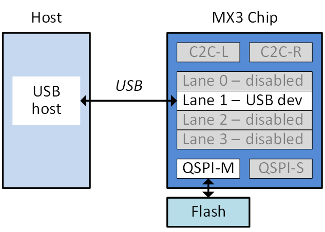
Figure 3 - Single Chip with USB
MX3 chip used in a single chip configuration, with a USB connection to the host, shall be set to this mode by bootstrapping CFG_MODE to 3’b110 (see Table 2). As illustrated in the figure, Lane 1 functions as a USB device connecting to the host, while Lane 0,2,3 are unused and thus disabled.
5.2 Single Chip with PCIe#
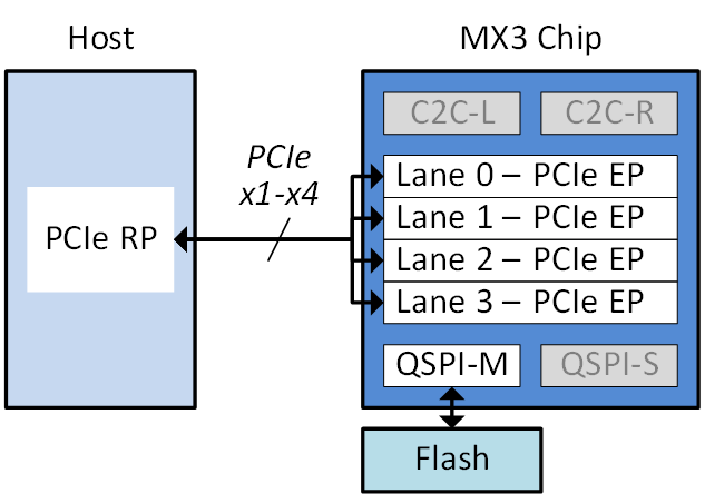
Figure 4 - Single Chip with PCIe
MX3 chip used in a single chip configuration, with a PCIe connection to the host, shall be set to this mode by bootstrapping CFG_MODE to 3’b010 (see Table 2). As illustrated in the figure, up to 2 lanes (Lane 0,1) can be used as a PCIe endpoint connecting to the host.
5.3 First Chip with USB#
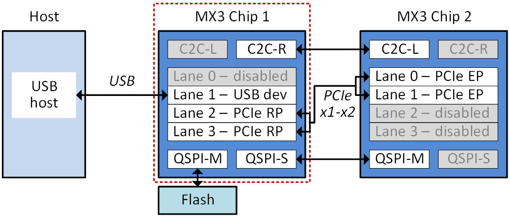
Figure 5 - First Chip with USB
MX3 chip used in a multi-chip configuration, with a USB connection to the host, shall be set to this mode by bootstrapping CFG_MODE to 3’b000 (see Table 2). As illustrated in the figure, Lane 1 functions as a USB device connecting to the host, up to 2 lanes (Lane 2,3) can be used as a PCIe root port connecting to the next MX3, and Lane 0 is unused and disabled.
5.4 First Chip with PCIe#
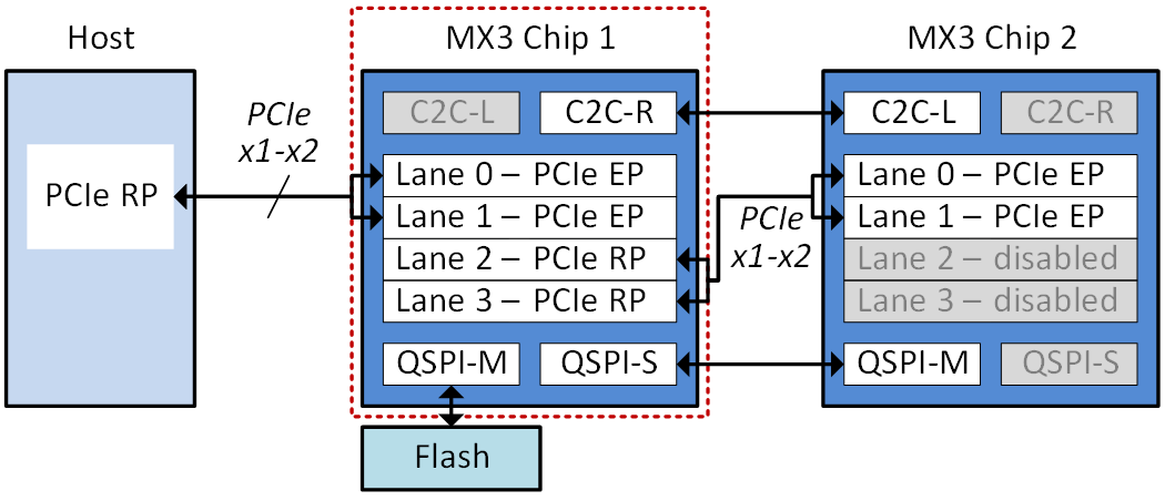
Figure 6 - First Chip with PCIe
MX3 chip used in a multi-chip configuration, with a PCIe connection to the host, shall be set to this mode by bootstrapping CFG_MODE to 3’b001 (see Table 2). As illustrated in the figure, up to 2 lanes (Lane 0,1) can be used as a PCIe endpoint connecting to the host, up to 2 lanes (Lane 2,3) can be used as a PCIe root port connecting to the next MX3.
5.5 Middle Chips#

Figure 7 - Middle Chips
MX3 chip used as one of the middle chips in a multi-chip configuration, shall be set to this mode by bootstrapping CFG_MODE to 3’b111 (see Table 2). As illustrated in the figure, up to 2 lanes (Lane 0,1) can be used as a PCIe endpoint connecting to the previous MX3, up to 2 lanes (Lane 2,3) can be used as a PCIe root port connecting to the next MX3.
5.6 Last Chip with Direct Host Connection#
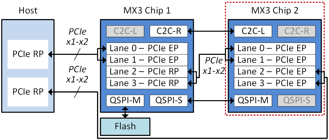
Figure 8 - Last Chip with Direct Host Connection
MX3 chip used as the last chip in a multi-chip configuration, shall be set to this mode by bootstrapping CFG_MODE to 3’b100 (see Table 2). As illustrated in the figure, up to 2 lanes (Lane 0,1) can be used as a PCIe endpoint connecting to the previous MX3, up to 2 lanes (Lane 2,3) can be used as a PCIe endpoint connecting to the host. Flash is optional if strap set to boot from PCIe, user can select boot from flash or from PCIe as needed.
5.7 Other Connectivity#
5.7.1 QSPI#
When equipped with a NOR Flash that has been programmed with MemryX’s image, the QSPI master interface will fetch from the Flash the ZSBL if bootstrap ZSBL_QSPI=1 (ZSBL from QSPI), and the firmware if bootstrap BOOT_MODE=00 (boot from QSPI). The QSPI slave interface is used for the MX3 chip to relay the ZSBL/firmware in multi-MX3 configurations. First chip boots from flash and the rest of the chips in cascade boot from PCIe.
5.7.2 Custom Chip-to-Chip Interface#
In multi-chip configurations, reset would be propagated and boot complete indication would be reflected backward while booting. Interrupts can be also exchanged between chips with our customed interface.
6. Power, Clocking and Reset#
6.1 Power Up Sequence#
The recommended power up sequence is to power up the rails as shown in the following figure. While there are NO specific requirements to sequence the IO, High Voltages it is recommended to power on the MPU_VDD_CORE, SOC_VDD_CORE after other power rails turned on (with a delay >= 500ns).
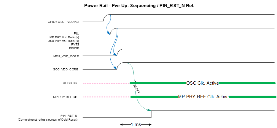
Figure 9 - Power Up and Cold Reset Timing Diagram
6.2 Power Down Sequence#
The recommended power down sequence is to power down the rails as shown in the following figure. There are NO specific requirements to power down the IO, High Voltages, and core rails. All can be turned off at the same instant.
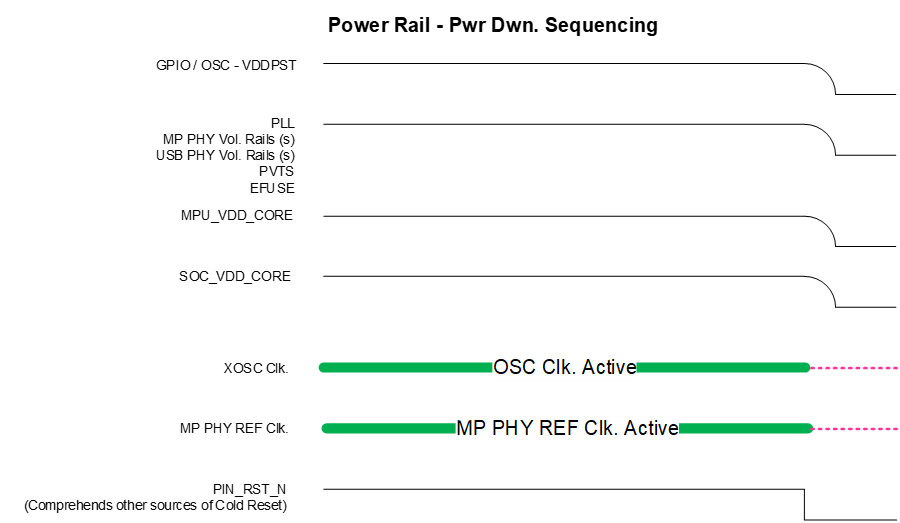
Figure 10 - Power Down Sequence
6.3 Clock Specifications#
The following table shows the clocking requirement for the MX3 chip. For detailed Xtal clock specification please refer to section 7.2.
Table 4 - Clocking Requirements
Clock Name |
Source |
Frequency |
Jitter/Tolerance |
|---|---|---|---|
OSC_XIN / OSC_XOUT |
Platform |
25MHz |
± 30 ppm |
CMN_REFCLK_P / CMN_REFCLK_M |
Platform |
100MHz |
± 300 ppm |
6.4 Reset Characteristics#
PIN_RST_N (COLD Reset that comprehends multiple sources on the platform) to be asserted for 1 ms (min.) upon availability of ALL power supplies (as depicted in Figure 9)
6.5 Power Modes#
6.5.1 Active Power Modes#
Three active power modes are defined for the user to select depending on the performance requirement and power/thermal budget of the applications.
Table 5 - Active Power Modes
Power Mode |
NPU Power Supply (VDD) |
NPU Frequency |
|---|---|---|
Low Power |
0.67V-0.70V |
200-600MHz |
Normal |
0.70V-0.79V |
650-850MHz |
Turbo |
0.81V-0.85V |
900-1000MHz |
In addition to selecting the appropriate power mode, limiting the MX3 ‘s FPS setting can significantly reduce power consumption. For example, the MX3 can run many models at greater than 100 FPS, however, some applications only require a lower FPS or may be limited by other components in the system, such as a 30 FPS camera. In addition to FPS there are other recipes to optimize active power like mapping the AI model to run on less chips and iteratively decreasing each active MX3’s NPU frequency.
6.5.2 Non-active Power Saving Modes#
Other than the active power modes described above, the MX3 offers power saving features to reduce power consumption when the MX3 is not actively processing data. These modes tradeoff power savings and exit latency (i.e. time from Power Savings to Active mode).
Hibernate Mode: In this mode the CPU clock frequency is decreased to 25 MHz. All other clocks are gated off, PLLs are programmed to their lowest power state, and NPU core groups are powered off, and PCIe Phy and Controller are set to ASPM L1.1 power state. During exit from this mode the NPU config DFP must be re-loaded when transitioning to active mode (“exit time”). The exit time can take about 50-100 ms depending on model parameters and host system capability. This mode provides the greatest power saving, but the exit time is longer than Standby Mode.
Standby Mode: In this mode the NPU remains on, but its clock is reduced to its lowest operating frequency (200 MHz). Since the NPU’s power rail remains on there is no need to re-load the NPU DFP configuration during transition to active mode. In Standby Mode the PCIe link operates in L1 substate (ASPM), USB 3.0 operates in U2/U3 low power states and low-speed peripheral clocks are disabled. This mode consumes more power than Hibernation Mode, but the exit latency is shorter.
Silicon power in non-active power saving modes and exit latency for both power modes are listed in below table.
Table 6 - Standby Power Modes
Power Saving Mode |
Power (mW) |
Exit Latency (ms) |
|---|---|---|
Standby Mode |
400 |
|
Hibernate Mode |
200 |
50 (Depends on Model) |
7. Electrical Specifications#
7.1 Operating Conditions#
The following table shows the operating conditions of all MX3 power rails. Note that three ranges are defined for the NPU power, each corresponding to a power mode. The voltage level of VDD can be adjusted based on the selected power mode. These voltages are at the MX3 chip pin and board design should allocate IR drop budget per PI analysis. System designers are recommended to use the typical voltage from the table below. For more information about power modes, please refer to Section 6.5.
Table 7 - Operating Conditions
Power Rail |
Description |
Voltage (V) |
||
Min |
Typical |
Max |
||
VDD_0P8V |
SoC power |
0.72 |
0.8 |
0.88 |
VDD |
NPU Power |
0.68 |
0.72 |
0.90 |
VDDA_PLL |
PLL power |
0.72 |
0.8 |
0.88 |
VDDA_PVT |
PVT sensor power |
1.62 |
1.8 |
1.98 |
USB_PHY_AVDD_CORE |
USB 2.0 PHY power |
0.76 |
0.8 |
0.88 |
USB_PHY_AVDD_IO_HV |
2.97 |
3.3 |
3.63 |
|
USB_PHY_AVDD_IO |
1.62 |
1.8 |
1.98 |
|
MP_PHY_AVDD_H |
PCIe Gen 3 & USB 3.1 PHY power |
1.08 |
1.2 |
1.98 |
MP_PHY_AVDD |
0.76 |
0.8 |
0.88 |
|
MP_PHY_AVDD_CLK |
0.76 |
0.8 |
0.88 |
|
EFUSE_VQPS |
E-fuse programming power |
1.71 |
1.8 |
1.89 |
VDDIO |
GPIO power |
1.62 |
1.8 |
1.98 |
VDDIO_OSC |
Internal oscillator pad power |
1.62 |
1.8 |
1.98 |
7.2 External Resistors#
The MX3 chip requires two external resistors for calibration purposes. Their requirements are shown in the following table.
Table 8 - Required External Resistors
Pin Name |
Value |
|---|---|
CMN_REXT |
An external resistor must be connected between this pin and the package ground. The resistance must be 3.01K Ohm with 1% tolerance. |
RTRIM |
An external resistor must be connected between this pin and the package ground. The resistance must be 500 Ohm with 1% tolerance. |
7.3 Crystal Oscillator#
Parameter |
Description |
Min |
Typ |
Max |
Unit |
Note |
|---|---|---|---|---|---|---|
fosc |
Crystal frequency |
25 |
MHz |
|||
tj_osc |
Frequency Tolerance |
± 30 |
PPM |
|||
CL |
Load Capacitance |
10 |
pF |
|||
Rr |
Equivalent Series Resistance |
100 |
Ω |
|||
DL |
Drive Level |
100 |
uW |
7.4 USB Electrical Characteristics#
Table 9 - USB3 Gen1 Data Rate Dependent Transmitter Parameters
Parameter |
Description |
Min |
Typ |
Max |
Unit |
Note |
|---|---|---|---|---|---|---|
tMIN-PULSE-Dj |
Deterministic min pulse |
0.96 |
UI |
|||
tMIN-PULSE-Tj |
Tx min pulse |
0.90 |
UI |
|||
tTX-EYE |
Transmitter Eye |
0.625 |
UI |
|||
tTX-DJ-DD |
Tx deterministic jitter |
0.205 |
UI |
|||
RTX-DC |
Transmitter DC common mode impedance |
18 |
30 |
Ω |
||
ITX-SHORT |
Transmitter short-circuit current limit |
60 |
mA |
|||
VTX-DC-CM |
Transmitter DC common-mode voltage |
0 |
2.2 |
V |
||
VTX-CM-AC-PPACTIVE |
Tx AC common mode voltage active |
100 |
mV(p-p) |
|||
VTX-CM-DC-ACTIVEIDLE-DELTA |
Absolute DC Common Mode Voltage between U1 and U0 |
200 |
mV |
|||
VTX-IDLE-DIFF-AC-PP |
Electrical Idle Differential Peak -Peak Output Voltage |
0 |
10 |
mV |
||
VTX-IDLE-DIFF-DC |
DC Electrical Idle Differential Output Voltage |
0 |
10 |
mV |
||
Tj |
TX total Jitter |
75 |
ps |
|||
Rj |
TX random Jitter |
2.42 |
Ps |
Table 10 - USB3 RX: receiver normative electrical parameters
Parameter |
Description |
Min |
Typ |
Max |
Unit |
Note |
|---|---|---|---|---|---|---|
UI (Gen1) |
Unit Interval |
199.94 |
200.06 |
UI |
||
RRX-DC |
Receiver DC common mode impedance |
18 |
30 |
Ω |
||
RRX-DIFF-DC |
DC differential impedance |
72 |
120 |
Ω |
||
ZRX-HIGH-IMP-DC-POS |
DC Input CM Input Impedance for V>0 during Reset or power down |
10k |
Ω |
|||
VRX-LFPS-DET-DIFFp-p |
LFPS Detect Threshold |
100 |
300 |
mA |
Table 11 - USB2 HS transmitter electrical parameters
Parameter |
Description |
Min |
Typ |
Max |
Unit |
Note |
|---|---|---|---|---|---|---|
THSDRAT |
Signal rate |
479.76 |
480.24 |
Mbps |
||
RER |
Rising edge rate |
2133 |
V/us |
|||
FER |
Falling edge rate |
2133 |
V/us |
|||
THSR |
Rise time |
300 |
ps |
|||
THSF |
Fall time |
300 |
ps |
|||
VHSTERM |
Idle time |
-20 |
20 |
mV |
||
VOL |
Low level |
-20 |
20 |
mV |
||
Dev CK |
Device chirp K |
-900 |
-500 |
mV |
||
Host CK |
Host chirp K |
-900 |
-500 |
mV |
||
Host CJ |
Host chirp J |
700 |
1100 |
mV |
||
EOPW |
EOP width |
7.5 |
8.5 |
bits |
Table 12 - USB2 HS receiver electrical parameters
Parameter |
Description |
Min |
Typ |
Max |
Unit |
Note |
|---|---|---|---|---|---|---|
VHSSQ |
Squelch detection threshold |
100 |
150 |
mV |
||
VHSDSC |
Disconnect detection threshold |
525 |
625 |
mV |
||
VHSCM |
Common mode range |
-50 |
500 |
mV |
||
VHSDI |
Different input sensitivity (Template 4) |
150 |
mV |
Table 13 - USB2 FS Transmitter Electrical Parameters
Parameter |
Description |
Min |
Typ |
Max |
Unit |
Note |
|---|---|---|---|---|---|---|
VOH |
High level (driven) |
2.8 |
3.6 |
V |
||
VOL |
Low level (idle) |
0.3 |
V |
|||
VOL |
Low level (driven) |
0.3 |
V |
|||
TFR |
Rise time (single end) |
4 |
20 |
ns |
||
TFF |
Fall time (single end) |
4 |
20 |
ns |
||
TFR |
Rise time (differential) |
4 |
20 |
ns |
||
TFF |
Fall time (differential) |
4 |
20 |
ns |
||
TFRFM |
Rise fall matching (differential) |
90 |
111.11 |
% |
||
TFDRATHS |
Signal rate |
11.994 |
12.006 |
Mbps |
||
VCRS |
Crossover voltage |
1.3 |
2 |
V |
||
TDJ1 |
Consecutive jitter |
-3500 |
3500 |
ps |
||
TDJ2 |
Paired JK jitter |
-4000 |
4000 |
ps |
||
TDJ2 |
Paired KJ jitter |
-4000 |
4000 |
ps |
||
TFEOPT |
EOP Width |
160 |
175 |
ns |
Table 14 - USB2 FS receiver electrical parameters
Parameter |
Description |
Min |
Typ |
Max |
Unit |
Note |
|---|---|---|---|---|---|---|
SERX threshold |
0.8 |
2 |
V |
|||
VCM |
Differential common mode range |
0.8 |
2.5 |
V |
||
TJR1 |
Jitter (to next transition) |
-18.5 |
18.5 |
ns |
||
TJR2 |
Jitter (paired transition) |
-9 |
9 |
ns |
||
TFEOPR |
Receiver SE0 interval of EOP |
82 |
ns |
|||
TFST |
Width of SE0 interval during differential transition |
14 |
ns |
Table 15 - USB2 LS transmitter electrical parameters
Parameter |
Description |
Min |
Typ |
Max |
Unit |
Note |
|---|---|---|---|---|---|---|
VOH |
High level (driven) |
2.8 |
3.6 |
V |
||
VOL |
Low level (idle) |
0.3 |
V |
|||
VOL |
Low level (driven) |
0.3 |
V |
|||
TR |
Rise time (single end) |
75 |
300 |
ns |
||
TF |
Fall time (single end) |
75 |
300 |
ns |
||
TLRFM |
Rise fall matching (single end) |
80 |
125 |
% |
||
TR |
Rise time (differential) |
75 |
300 |
ns |
||
TF |
Fall time (differential) |
75 |
300 |
ns |
||
TLRFM |
Rise fall matching (differential) |
80 |
125 |
% |
||
TLDRATHS |
Signal rate |
1.49925 |
1.50075 |
Mbps |
||
VCRS |
Crossover voltage |
1.3 |
2 |
V |
||
Consecutive Jitter-Up |
Consecutive Jitter (upstream) |
-95 |
95 |
ns |
||
Paired JK Jitter-Up |
Paired JK Jitter (upstream) |
-150 |
150 |
ns |
||
Paired KJ Jitter-Up |
Paired KJ Jitter (upstream) |
-150 |
150 |
ns |
||
Consecutive Jitter-Down |
Consecutive Jitter (downstream) |
-71 |
71 |
ns |
||
Paired JK Jitter-Down |
Paired JK Jitter (downstream) |
-44 |
44 |
ns |
||
Paired KJ Jitter-Down |
Paired KJ Jitter (downstream) |
-44 |
44 |
ns |
||
TLEOPT |
EOP width |
1.25 |
1.5 |
ns |
Table 16 - USB2 LS receiver electrical parameters
Parameter |
Description |
Min |
Typ |
Max |
Unit |
Note |
|---|---|---|---|---|---|---|
SERX threshold |
0.8 |
2 |
V |
|||
VCM |
Differential common mode range |
0.8 |
2.5 |
V |
||
TJR1 |
Jitter (to next transition) |
-152 |
152 |
ns |
||
TJR2 |
Jitter (paired transition) |
-200 |
-200 |
ns |
||
TFEOPR |
Receiver SE0 interval of EOP |
670 |
ns |
|||
TLST |
Width of SE0 interval during differential transition |
210 |
ns |
7.5 PCIe Electrical Characteristics#
Table 17 - PCIe Gen1 Data Rate Dependent Transmitter Parameters
Parameter |
Description |
Min |
Typ |
Max |
Unit |
Note |
|---|---|---|---|---|---|---|
UI |
Unit Interval |
399.88 |
400.12 |
ps |
||
VTX-DIFF-PP |
Differential peak-peak Tx voltage swing for full swing operation |
800 |
1200 |
mV |
||
VTX-DIFF-PP-LOW |
Differential peak-peak Tx voltage swing for low swing operation |
400 |
1200 |
mV |
||
VTX-EIEOS-FS |
Tx deemphasis ratio for 2.5 and 5.0 GT/s |
-4.5 |
-2.5 |
dB |
||
TTX-UTJ |
Tx uncorrelated total jitter |
100 |
ps PP at 10-12 |
|||
TTX-UDJDD |
Tx uncorrelated Dj for nonembedded Refclk |
100 |
ps PP |
|||
LTX-SKEW |
Lane-to-Lane Output Skew |
2.5 |
ns |
Table 18 - PCIe Gen2 Data Rate Dependent Transmitter Parameters
Parameter |
Description |
Min |
Typ |
Max |
Unit |
Note |
|---|---|---|---|---|---|---|
UI |
Unit Interval |
199.94 |
200.06 |
ps |
200.00 |
|
VTX-DIFF-PP |
Differential peak-peak Tx voltage swing for full swing operation |
800 |
1200 |
mV |
||
VTX-DIFF-PP-LOW |
Differential peak-peak Tx voltage swing for low swing operation |
400 |
1200 |
mV |
||
VTX-DE-RATIO-3.5dB |
Tx deemphasis ratio for 2.5 and 5.0 GT/s |
-4.5 |
-2.5 |
dB |
||
VTX-DE-RATIO-6dB |
Tx deemphasis ratio for 5.0 GT/s |
-7.5 |
-4.5 |
dB |
-4.86 |
|
TTX-UTJ |
Tx uncorrelated total jitter |
50 |
ps PP at 10-12 |
|||
TTX-UDJDD |
Tx uncorrelated Dj for nonembedded Refclk |
30 |
ps PP |
|||
TTX-UPW-TJ |
Total uncorrelated pulse width jitter |
40 |
ps PP at 10-12 |
|||
TTX-UPWDJDD |
Deterministic DjDD uncorrelated pulse width jitter |
40 |
ps PP |
|||
LTX-SKEW |
Lane-to-Lane Output Skew |
2.0 |
ns |
Table 19 - PCIe Gen3 Data Rate Dependent Transmitter Parameters
Parameter |
Description |
Min |
Typ |
Max |
Unit |
Note |
|---|---|---|---|---|---|---|
UI |
Unit Interval |
124.9625 |
125.0375 |
ps |
||
VTX-DIFF-PP |
Differential peak-peak Tx voltage swing for full swing operation |
800 |
1300 |
mV |
||
VTX-DIFF-PP-LOW |
Differential peak-peak Tx voltage swing for low swing operation |
400 |
1300 |
mV |
||
VTX-EIEOS-FS |
Minimum voltage swing during EIEOS for full swing signaling |
250 |
mV-PP |
|||
VTX-EIEOS-RS |
Minimum voltage swing during EIEOS for reduces swing signaling |
232 |
mV-PP |
|||
VTX-BOOST-FS |
Maximum nominal Tx boost ratio for full swing |
-8.0 |
dB |
|||
VTX-BOOST-RS |
Maximum nominal Tx boost ratio for reduced swing |
-2.5 |
dB |
|||
EQTX-COEFF-RES |
Tx coefficient resolution |
1/63 |
1/24 |
N/A |
||
TTX-UTJ |
Tx uncorrelated total jitter |
31.25 |
ps PP at 10-12 |
|||
TTX-UDJDD |
Tx uncorrelated Dj for nonembedded Refclk |
12 |
ps PP |
|||
TTX-UPW-TJ |
Total uncorrelated pulse width jitter |
24 |
ps PP at 10-12 |
|||
TTX-UPWDJDD |
Deterministic DjDD uncorrelated pulse width jitter |
10 |
ps PP |
|||
LTX-SKEW |
Lane-to-Lane Output Skew |
1.5 |
ns |
Table 20 - PCIe transmitter data rate independent transmitter characteristics
Parameter |
Description |
Min |
Typ |
Max |
Unit |
Note |
|---|---|---|---|---|---|---|
VTX-AC-CM-PP |
Tx AC peak-peak common mode voltage |
150 |
mV-PP |
|||
VTX-DC-CM |
Tx DC peak-peak common mode voltage |
0 |
3.6 |
V |
||
VTX-CM-DC-ACTIVEIDLE-DELTA |
Absolute delta of DC Common Mode Voltage during L0 and Electrical Idle |
0 |
100 |
mV |
||
VTX-CM-DC-LINEDELTA |
Absolute Delta of DC Common Mode Voltage between D+ and D- |
0 |
25 |
mV |
||
VTX-IDLE-DIFF-AC-p |
Electrical Idle Differential Peak Output Voltage |
0 |
20 |
mV |
||
VTX-IDLE-DIFF-DC |
DC Electrical Idle Differential Output Voltage |
0 |
5 |
mV |
||
VTX-RCV-DETECT |
The amount of voltage change allowed during Receiver detection |
600 |
mV |
|||
ZTX-DIFF-DC |
DC differential Tx impedance |
120 |
Ω |
75.2 |
Table 21 - PCIe RX termination measurement results
Parameter |
Description |
Min |
Typ |
Max |
Unit |
Note |
|---|---|---|---|---|---|---|
ZRX-DC |
Receiver DC single ended impedance |
40 |
60 |
Ω |
||
ZRX-HIGH-IMP-DC-POS |
DC input CM input impedance for V≥0 during Reset or power-down |
≥10K (0-200mV) |
Ω |
|||
ZRX-HIGH-IMP-DC-POS |
DC input CM input impedance for V≥0 during Reset or power-down |
≥20K (>200mV) |
Ω |
|||
ZRX-HIGH-IMP-DC-NEG |
DC input CM input impedance for V<0 during Reset or power-down |
1.0K |
Ω |
7.6 Regular GPIO DC characteristics#
Table 22 - GPIO PAD electrical characteristics
Parameter |
Description |
Min |
Typ |
Max |
Unit |
Note |
|
|---|---|---|---|---|---|---|---|
VIL |
Input Low Voltage |
-0.3 |
0.3*VDDIO |
V |
|||
VIH |
Input High Voltage |
0.65*VDDIO |
VDDIO+0.3 |
V |
|||
VT |
Threshold Point |
0.83 |
0.92 |
1.01 |
V |
||
VT+ |
Schmitt Trigger Low to High Threshold Point |
0.99 |
1.1 |
1.21 |
V |
||
VT- |
Schmitt Trigger High to Low Threshold Point |
0.74 |
0.85 |
0.9 |
V |
||
VTPU |
Threshold Point with Pull-up Resistor Enabled |
0.82 |
0.91 |
1 |
V |
||
VTPD |
Threshold Point with Pull-down Resistor Enabled |
0.84 |
0.93 |
1.02 |
V |
||
VTPU+ |
Schmitt Trigger Low to High Threshold Point with Pull-up Resistor Enabled |
0.98 |
1.09 |
1.2 |
V |
||
VTPU- |
Schmitt Trigger High to Low Threshold Point with Pull-up Resistor Enabled |
0.73 |
0.81 |
0.89 |
V |
||
VTPD+ |
Schmitt Trigger Low to High Threshold Point with Pull-down Resistor Enabled |
1 |
1.11 |
1.22 |
V |
||
VTPD- |
Schmitt Trigger High to Low Threshold Point with Pull-down Resistor Enabled |
0.75 |
0.83 |
0.91 |
V |
||
VTSPU |
Threshold Point with Strong Pull-up Resistor Enabled |
0.78 |
0.86 |
0.94 |
V |
||
VTSPU+ |
Schmitt Trigger Low to High Threshold Point with Strong Pull-up Resistor Enabled |
0.95 |
1.05 |
1.15 |
V |
||
VTSPU- |
Schmitt Trigger High to Low Threshold Point with Strong Pull-up Resistor Enabled |
0.68 |
0.76 |
0.83 |
V |
||
I |
Input Leakage Current @ VI=1.8V or 0V |
±10μ |
A |
||||
IOZ |
Tri-state Output Leakage Current @ VO=1.8V or 0V |
±10μ |
pF |
||||
RSPU |
Strong Pull-up Resistor |
2.8k |
3.5k |
4.5k |
Ω |
||
RPU |
Pull-up Resistor |
18k |
25k |
38k |
Ω |
||
RPD |
Pull-down Resistor |
17k |
22k |
33k |
Ω |
||
VOL |
Output Low Voltage |
0.45 |
V |
||||
VOH |
Output High Voltage |
VDDIO-0.45 |
V |
||||
IOL |
IOL Low Level Output Current @VOL (max) |
DS=0 |
2.1 |
3.1 |
4.1 |
mA |
|
DS=1 |
4.6 |
6.7 |
8.9 |
mA |
|||
DS=2 |
6.6 |
9.6 |
12.8 |
mA |
|||
DS=3 |
8.8 |
12.9 |
17.2 |
mA |
|||
DS=4 |
12.2 |
18 |
24 |
mA |
|||
DS=5 |
14.2 |
21 |
28 |
mA |
|||
DS=6 |
15.7 |
23.3 |
31.1 |
mA |
|||
DS=7 |
17.5 |
26 |
34.8 |
mA |
|||
DS=8 |
23.1 |
34.4 |
46.2 |
mA |
|||
DS=9 |
24.4 |
36.5 |
49 |
mA |
|||
DS=10 |
25.4 |
38 |
51 |
mA |
|||
DS=11 |
26.6 |
39.8 |
53.5 |
mA |
|||
DS=12 |
28.3 |
42.2 |
56.6 |
mA |
|||
DS=13 |
29.4 |
43.9 |
58.9 |
mA |
|||
DS=14 |
30.2 |
45.1 |
60.5 |
mA |
|||
DS=15 |
31.2 |
46.6 |
62.6 |
mA |
|||
IOH |
IOH High Level Output Current @VOH (max) |
DS=0 |
1.8 |
2.8 |
3.8 |
mA |
|
DS=1 |
3.9 |
5.9 |
8.1 |
mA |
|||
DS=2 |
5.5 |
8.4 |
11.6 |
mA |
|||
DS=3 |
7.4 |
11.3 |
15.6 |
mA |
|||
DS=4 |
10.2 |
15.7 |
21.6 |
mA |
|||
DS=5 |
11.9 |
18.3 |
25.1 |
mA |
|||
DS=6 |
13.1 |
20.2 |
27.9 |
mA |
|||
DS=7 |
14.6 |
22.6 |
31.2 |
mA |
|||
DS=8 |
19.2 |
29.9 |
41.4 |
mA |
|||
DS=9 |
20.4 |
31.6 |
44 |
mA |
|||
DS=10 |
21.2 |
33 |
45.8 |
mA |
|||
DS=11 |
22.2 |
34.6 |
48.1 |
mA |
|||
DS=12 |
23.6 |
36.7 |
50.9 |
mA |
|||
DS=13 |
24.5 |
38.2 |
53 |
mA |
|||
DS=14 |
25.2 |
39.2 |
54.4 |
mA |
|||
DS=15 |
26 |
40.5 |
56.3 |
mA |
|||
7.7 Power Consumption#
The power rail group of MX3 silicon is listed below along with maximum current rating. Current consumption of each power rail depends on model type, video frame rate (fps) and frequency of operation. However max current rating listed in table below will guide designer to select power management components for MX3 based hardware.
Sr. No. |
Power Rail Group |
Voltage (V) |
Type |
Max Current |
|
|---|---|---|---|---|---|
1 |
VDD_0P8V & VDDA_PLL |
0.8 |
Digital |
450 mA |
|
2 |
VDD |
0.70 - 0.9 |
Digital |
0.8 - 12.5 A |
|
3 |
USB2_PHY_AVDD_CORE |
0.8 |
Analog |
20 mA |
|
MP_PHY_AVDD (1/2) MP_PHY_AVDD_CLK |
0.8 |
Analog |
350 mA |
||
4 |
USB2_PHY_AVDD_IO_HV |
3.3 | Analog |
3.75 mA |
||
5 |
USB2_PHY_AVDD_IO |
1.8 |
Analog |
6.50 mA |
|
VDDA_PVT (1/2/3/4) |
1.8 |
Analog |
2.5 mA |
||
6 |
MP_PHY_AVDD_H |
1.2 |
Analog |
25 mA |
|
7 |
EFUSE_VQPS |
1.8 |
Digital |
70 mA |
|
VDDIO VDDIO_OSC |
1.8 |
Digital |
Depends on Drive Strength |
||
In active mode operation, the power consumption depends on the AI model, the power mode, and the FPS.
8. Mechanical and Thermal Specifications#
8.1 Package Information#
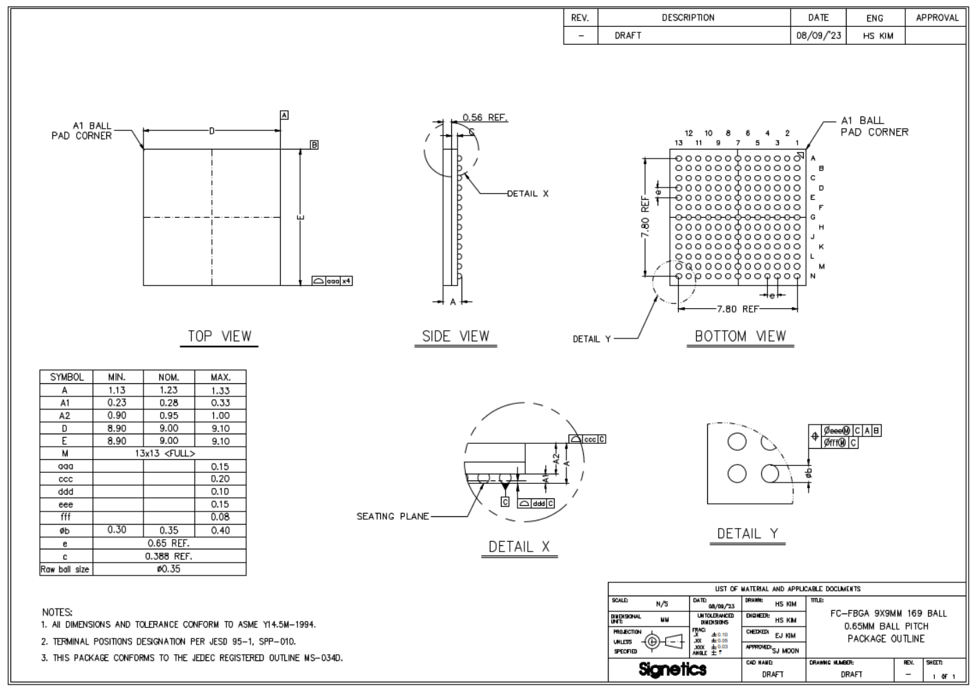
Figure 11 - Package Outline Drawing
8.2. Thermal Information#
MX3 package thermal characteristics were simulated and tested based on boundary conditions defined by JEDEC standards EIA/JESD51-2, EIA/JESD51-6, EIA/JESD51-8 and EIA/JESD51-9. Thermal characteristic simulation and validation testing used 1.6 mm thick 4-layer PCB. Thermal resistance of MX3 package is listed in “Thermal Resistance Characteristics” table.
Table 24 - Thermal Resistance Characteristics
Package |
Airflow |
θJA (°C/W) |
θJB (°C/W) |
|---|---|---|---|
169 Ball FC-FBGA 9mm x 9mm |
0 m/s (No airflow) |
19.88 |
TBD |
8.3. Reflow Profile#
The MSL (Moisture Sensitivity Level) is 3.
The reflow profile follows the standard specified in J-STD-020.
Peak Reflow Temperature Tc = 260°C (package thickness <1.6mm).
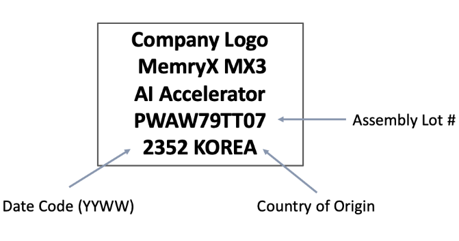
8.4. Part Marking#
9. Ordering Information#
Table 25 - Ordering Information
Part Name |
Part Number |
Description |
|---|---|---|
MemryX MX3 AI Accelerator |
MX3-1 |
AI Accelerator IC |
10. Glossary#
Abbreviation |
Description |
|---|---|
ASPM |
Active State Power Management |
BF16 |
16-bit Floating Point Format |
BS |
Boot Strap |
CMOS |
Complementary Metal-Oxide |
CS |
Chip Select |
DDR |
Double Data Rate |
DNN |
Deep Neural Network |
DMA |
Direct Memory Access |
ECC |
Error Correction Code |
FP |
Floating Point |
GPIO |
General Purpose Input Output |
GT |
Giga-Transfers |
HS |
High Speed |
I/O |
Input Output |
I2C |
Inter-Integrated Circuit |
INT |
Integer Format |
MCU |
Microcontroller Unit |
NPU |
Neural Processing Unit |
MSL |
Moisture Sensitivity Level |
NN |
Neural Network |
PCIe |
Peripheral Component Interconnect Express |
PLL |
Phase Locked Loop |
PVT |
Process, Voltage, Temperature |
QSPI |
Quad Serial Peripheral Interface |
RGB |
Red, Green, Blue |
ROM |
Read Only Memory |
RX |
Receiver |
SDR |
Single Data Rate |
SoC |
System on Chip |
SRAM |
Static Random Access Memory |
SS |
Slow Speed |
SSP |
Synchronous Serial Port |
TOPS |
Tera Operations per Second |
TX |
Transmitter |
UART |
Universal Asynchronous Receiver |
USB |
Universal Serial Bus |
XTAL |
Quartz Crystal |
YUV |
Analog Color TV standard |
ZSBL |
Zero Stage Boot Loader |
11 Disclaimer and Notices#
11.1 Copyright#
Copyright © 2024 MemryX Inc.
Published under the Creative Commons No-Derivates (CC-BY-ND) license.
11.2 General Notices#
To the fullest extent permitted by law, MemryX provides this document “as is” and disclaims all warranties, either express or implied, statutory, or otherwise, including but not limited to the warranties of merchantability, non-infringement of third-party rights, and fitness for particular purposes.
This document may inadvertently contain technical inaccuracies or other errors. MemryX assumes no liability for any such errors and for damages, whether direct, indirect, incidental, consequential, or otherwise, that may result from such errors, including but not limited to loss of data or profits.
The content in this document is subject to change without notice. MemryX reserves the right to make changes to document content without notification to users.

