MemryX MX3 M.2 AI Accelerator Module Datasheet#
1. Introduction#
This datasheet details the design and configuration of MemryX’s MX3 M.2 AI Acceleration Module (hereafter referred to as M.2 Module). Below is a table showing the specifications of the M.2 Module. More details are covered in later sections.
SYSTEM |
|
AI Processor |
MemryX MX3 (x4) |
Host Processor Support |
ARM, x86, RISC-V |
ELECTRICAL |
|
Input Voltage |
3.3V ± 5% |
Interface |
PCIe Gen 3, 2-lanes |
MECHANICAL |
|
Form Factor |
M.2-2280-D5-M, Socket 3 |
Dimensions |
3.15” x 0.87” (22 mm x 80 mm) |
ENVIRONMENTAL |
|
Operating Temperature |
-40° to +85° C |
COMPLIANCE |
|
Certification |
CE / FCC Class A, RoHS |
2. Form Factor#
The M.2 Module is designed to be compliant with M.2-2280-D5-M form factor defined in the specification. Refer to Figure 1 and 2 for the nomenclature and actual board picture/size.
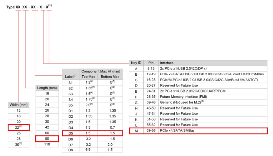
Figure 1 – M.2 Module Nomenclature
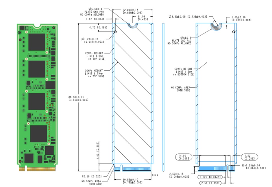
Figure 2 – M.2 Module Mechanical Outline
3. Placement#
The following picture shows the placement of key components/interfaces on the M.2 Module (power components are excluded). The function of each component/interface will be described in later chapters.
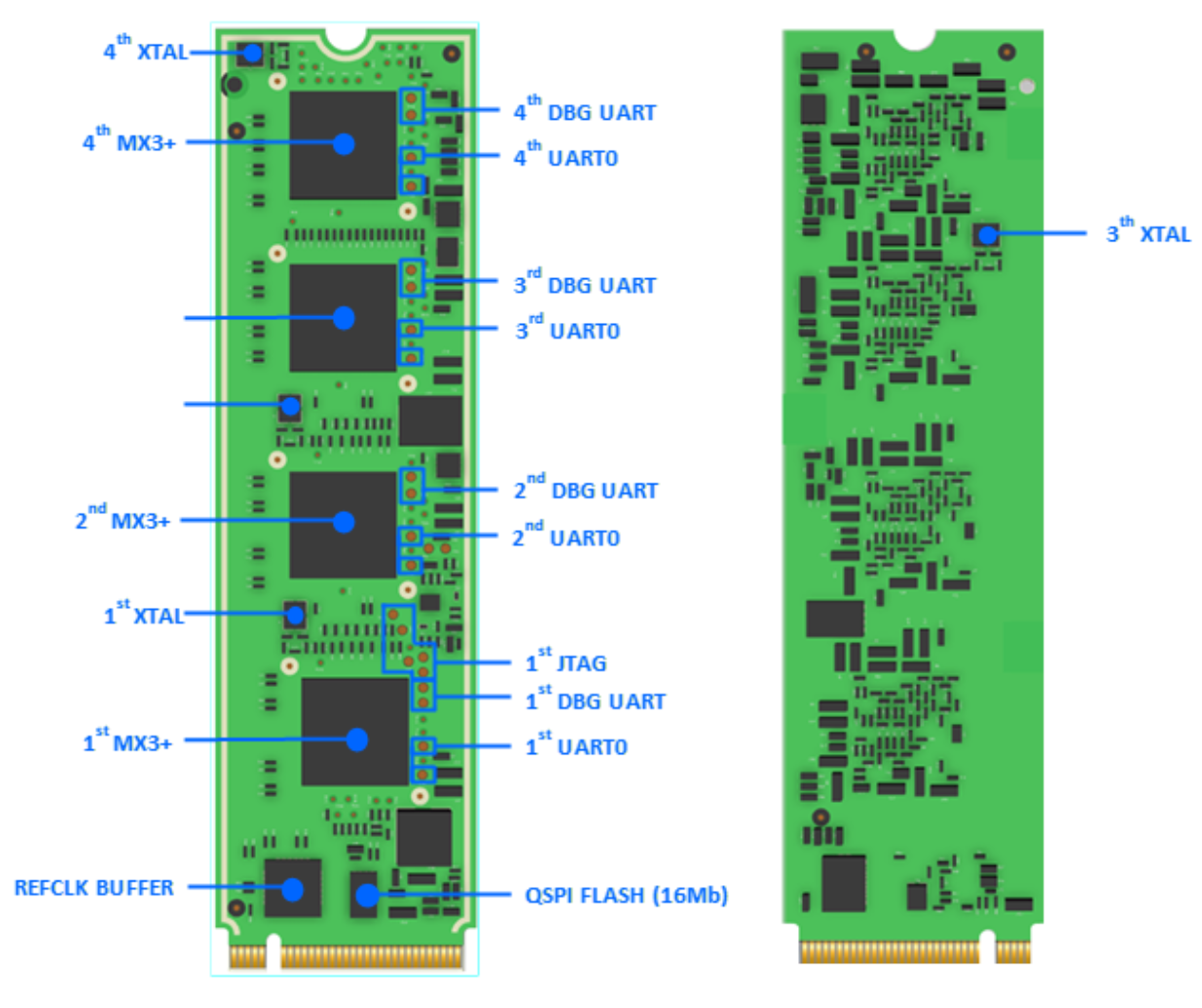
Figure 3 – M.2 Module Components Placement
4. Pin Definition#
This pinout table and I/O direction is defined from the module’s perspective, not the baseboard perspective. Pin definition is compatible with PCI-SIG M.2 specification for M-key applications.
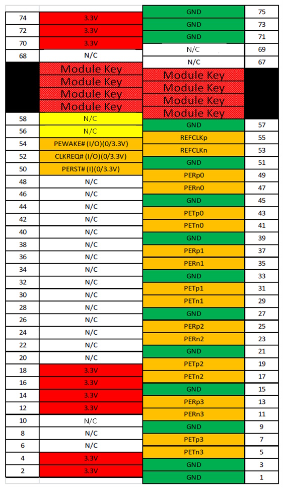
Figure 4 – M.2 Module Pinout Table
Interface |
Signal Name |
I/O |
Description |
|
|---|---|---|---|---|
Power Ground |
3.3V (9 pins) |
I |
3.3V running power source. |
|
GND (15 pins) |
Ground. |
|||
PCIe |
PETp0/PETn0 |
O |
PCIe TX/RX Differential signals defined by the PCIe 3.0 specification. The TX/RX are defined on module perspective. PET is TX on module and connects to RX on host. PER is RX on module and connects to TX on host. |
|
PETp1/PETn1 |
O |
|||
PETp2/PETn2 |
O |
|||
PETp3/PETn3 |
O |
|||
PERp0/PERn0 |
I |
|||
PERp1/PERn1 |
I |
|||
PERp2/PERn2 |
I |
|||
PERp3/PERn3 |
I |
|||
REFCLKp/REFCLKn |
I |
PCIe Reference Clock signals (100 MHz) defined by the PCIe 3.0 specification |
||
PERST# |
I |
PE-Reset is a functional reset to the card as defined by the PCI Express CEM Rv3.0 |
||
CLKREQ# |
O |
Clock Request is a reference clock request signal as defined by the PCIe Mini CEM specification; Open Drain with pull up on Platform; Active Low. |
||
PEWAKE# |
O |
Signal for waking up the host system. |
||
Table 2. M.2 Module Pinout Description
5. Block Diagram#
Below is the block diagram of the M.2 Module.

Figure 5 – M.2 Module Block Diagram
6. Power Design Constraint#
There are two power constraint numbers listed in the M.2 specification. M.2 Module is designed to fulfill the maximum power requirement which host can provide.
Constraint from PCIe M.2 Spec |
Current |
Total Power Allowed |
|---|---|---|
Power rating table |
3500 mA |
11.55W |
Adaptor power section |
4500 mA (500mA/pin) |
14.85W |
Table 3. Current Constraint Table
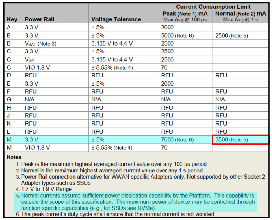
Figure 6 – Power Rating Table for M.2 Add-in Cards (PCI Express M.2 Specification Rev 3.0)
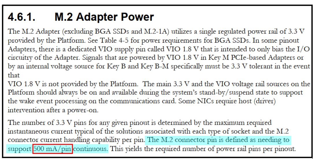
Figure 7 – M.2 Adapter Power (PCI Express M.2 Specification Rev 3.0)
7. Power Distribution#
There are 4 different power rails on a single MX3 chip which the board design should provide. Power solution types have been selected based on the current consumption of each rail. Table 4 shows the total power consumption of the M.2 Module when running a certain model.
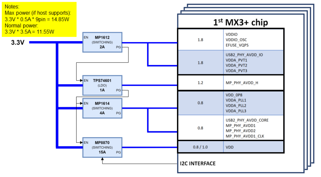
Figure 8 - Power Distribution
Board Power Calculation Table |
||||||||||
Design Model: M.2 Module |
PS
Design
|
|||||||||
Input Voltage |
3.3 |
3.3 |
3.3 |
3.3 |
3.3 |
V |
||||
Output Voltage |
0.75 |
0.8 |
1.2 |
1.8 |
3.3 |
V |
||||
Components |
Qty |
MPU0P8V |
CorePWR |
PCIE_PHY |
VCC1P8V |
VCC3P3V |
||||
MX3 |
USB2 |
0 |
0 |
0 |
0 |
0 |
0 |
A |
0.00 |
|
IO |
4 |
0 |
0 |
0 |
0.11 |
0 |
A |
0.80 |
||
eFuse |
4 |
0 |
0 |
0 |
0.07 |
0 |
A |
0.50 |
||
PVTS |
4 |
0 |
0 |
0 |
0.0026312 |
0 |
A |
0.02 |
||
PLL |
4 |
0 |
0.015 |
0 |
0 |
0 |
A |
0.05 |
||
PCIe3 (USB3) |
MP_PHY_AVDD_H |
4 |
0 |
0 |
0.01414 |
0 |
0 |
A |
0.07 |
|
MP_PHY_AVDD1/2 |
4 |
0 |
0.23923 |
0 |
0 |
0 |
A |
0.77 |
||
MP_PHY_AVDD1_CLK |
4 |
0 |
0.11136 |
0 |
0 |
0 |
A |
0.36 |
||
NPU |
VDD |
4 |
3.257 |
0 |
0 |
0 |
0 |
A |
9.77 |
|
Core |
VDD_0P8 |
4 |
0 |
0.1875 |
0 |
0 |
0 |
A |
0.60 |
|
QSPI Flash |
1 |
0 |
0 |
0 |
0.02 |
0 |
A |
0.04 |
||
Level Shifter |
1 |
0 |
0 |
0 |
0 |
0.064 |
A |
0.00 |
||
Clock Buffer |
1 |
0 |
0 |
0 |
0 |
0.035 |
A |
0.00 |
||
12.97 |
||||||||||
Load Current |
13.028 |
2.212 |
0.057 |
0.755 |
0.099 |
A |
||||
Load Power |
9.77 |
1.77 |
0.07 |
1.36 |
0.33 |
W |
||||
Total Max Load Power |
W |
12.97 |
||||||||
Power Solution |
Switching |
Switching |
LDO |
Switching |
N/A |
||
|---|---|---|---|---|---|---|---|
Power Supply Efficiency |
88% |
85% |
36% |
92% |
100% |
% |
|
Input Power - Max |
11.10 |
2.08 |
0.19 |
1.48 |
0.33 |
W |
14.85 |
Table 4. M.2 Module Power Consumption Table
8. Power Sequence#
This section details the power sequence requirements specified in the M.2 spec.
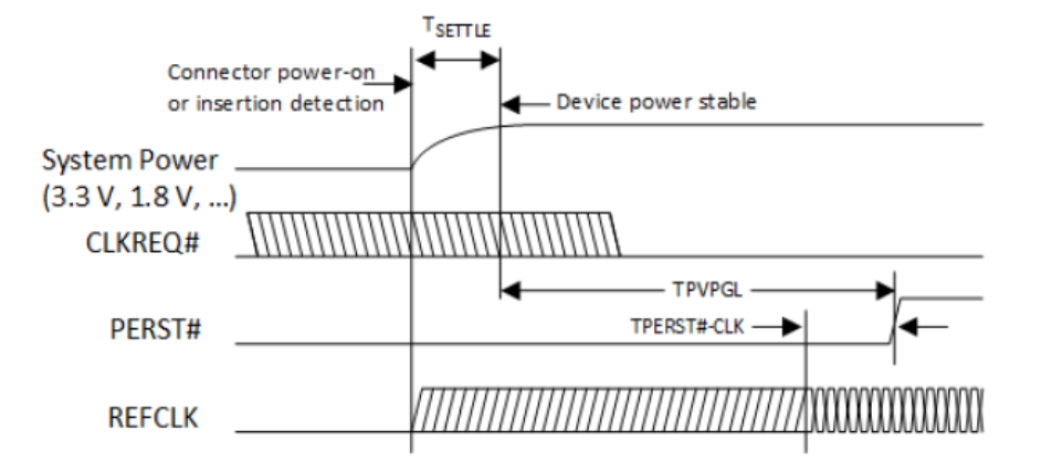
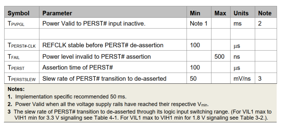
Figure 9 - PCIe Power Up Timing (from PCI Express M.2 Specification Rev 3.0).
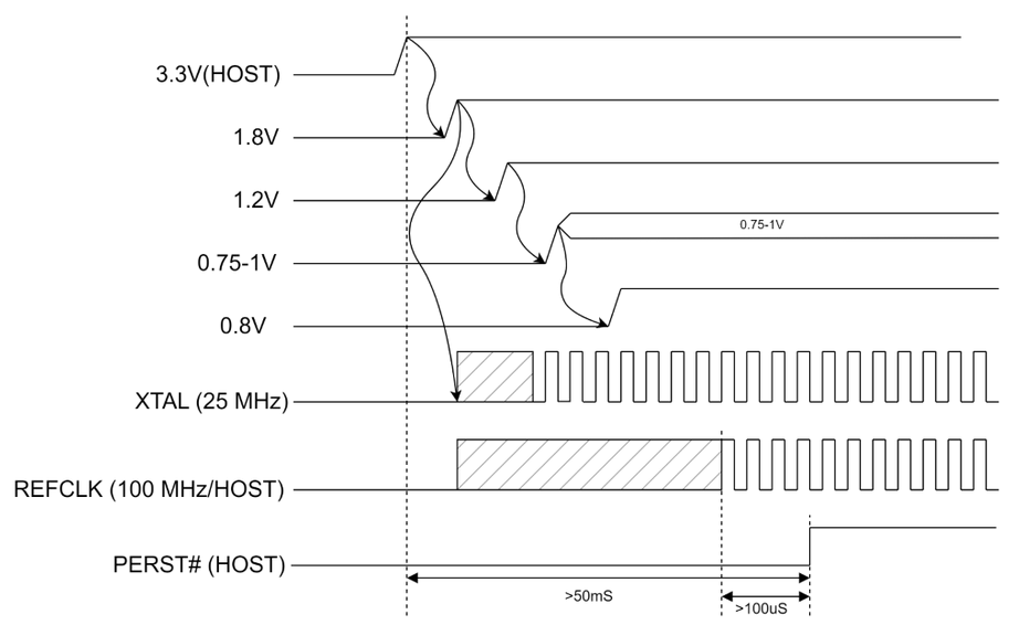
Figure 10 - M.2 Module Power Up Timing Diagram
9. Key Features#
9.1 PCIe#
In normal operation, Chip 1 receives input (video or image stream for CV applications) data from the external Host processor via a PCIe connection. The Host processor expects an inference result in return. The 4 MX3 chips appear as one logical unit to the NeuralCompiler and runtime software stack, running only a 4-chip DFP.


Figure 11 - Chip Cascade Connection through PCIe
9.2 Clocks#
There’re two clock sources required by MX3 chip:
25MHz clock from local XTALs.
100MHz REFCLK from host through 1:4 fan-out buffer.

Figure 12 - Clock Source For Single Chip

Figure 13 - Clock Source From HOST
9.3 Flash (Optional)#
Connected to Chip 1 is an optional external flash memory via QSPI interface. It is used to store AI Model parameters and Boot Code. The MX3 also has the capability to boot from PCIe interface.

Figure 14 - QSPI Interface
9.4 Straps#
There are 15 strap pins on each MX3 chip for selection of operating modes. The following table shows the default settings of the strap pins on M.2 Module for each chip to meet the requirement of cascade configuration.
Strap Number |
Strap Name |
Pin Shared |
Strap Description |
Internal
PU/PD
|
Chip1 |
Chip2 |
Chip3 |
Chip4 |
0 |
TEST_MODE |
CR_INTR_ACK_OUT |
Enables test mode for the SoC.
1’b0 : Mission Mode
1’b1 : Test Mode
|
PD |
0 |
0 |
0 |
0 |
1 |
BISR_BY_PASS |
CR_INTR_OUT |
Enables BISR by pass mode.
1’b0 : BISR enabled.
1’b1 : BISR by pass.
|
PD |
1 |
1 |
1 |
1 |
2 |
BOOT_HALT |
CL_INTR_ACK_OUT |
1’b0 : Boot NOT Halted
1’b1 : Boot Halted
|
PD |
0 |
0 |
0 |
0 |
3 |
ZSBL_QSPI |
CL_INTR_OUT |
1’b0 : ROM : ZSBL
1’b1 : QSPI : ZSBL
|
PD |
0 |
0 |
0 |
0 |
4 |
CFG_MODE |
|
Defines the configuration mode for Huron ASIC.
3’b000 : Mode 1 - 1st Chip - USB Host / Chained
3’b001 : Mode 2 - 1st Chip - PCIe Host / Chained
3’b010 : Mode 3 - Single Chip - PCIe Host
3’b011 : Mode 4 - 1st Chip - USB & PCIe Host EP / Chained RP
3’b100 : Mode 5 - Last Chip
3’b101 : Mode 6 - Single Chip - USB Host
3’b110 : Mode 7 - Legacy USB
3’b111 : Mode 8 - Middle of Chain
|
PU |
1 |
1 |
1 |
0 |
5 |
PD |
0 |
1 |
1 |
0 |
|||
6 |
PD |
0 |
1 |
1 |
1 |
|||
7 |
BOOT_MODE |
|
Defines the boot mode for MX3
2’b00 : QSPI
2’b01 : USB
2’b10 : PCIe
2’b11 : UART
|
PD |
0 |
0 |
0 |
0 |
8 |
PU |
1 |
1 |
1 |
1 |
|||
9 |
GPIO_MPU_FC |
GPIO [12] |
1’b0: NPU flow control through GPIO.
1’b1 : NPU flow control through PCIe.
|
PD |
1 |
1 |
1 |
1 |
10 |
PLT_BOOT_SEQ_DEP |
GPIO [13] |
1’b0 : Chip N does not influences Chip N + 1 boot.
1’b1 : Chip N influences Chip N + 1 boot.
|
PD |
1 |
1 |
1 |
0 |
11 |
PLT_PCIE_CLK_MODE |
GPIO [14] |
1’b0 : PCIE SS common clocking mode.
1’b1 : PCIE SS non common clocking mode.
|
PD |
0 |
0 |
0 |
0 |
12 |
Spare 1 |
GPIO [15] |
Spare 1
Prim. XIN if SYS_OSC_BP (CL_BOOT_COMP_OUT strap is set (to 1)
|
PD |
0 |
0 |
0 |
0 |
13 |
SYS_OSC_BP |
CL_BOOT_COMP_OUT |
1’b0 : OSC PAD Used as XIN
1’b1 : GPIO [15] Used as XIN
|
PD |
0 |
0 |
0 |
0 |
Table 5. M.2 Module Strap Setting Table
9.5 I2C#
Each MX3 is equipped with an I2C interface (master). Only 1st MX3 I2C interface is implemented on M.2 Module. The main purpose of the I2C interface of 1st MX3 chip is to control PMIC output voltage for NPU power rail. The output voltage can be selected (ranging from 0.7V to 1V) to meet different power mode requirements by writing to the I2C registers.

Figure 15 - I2C Interface Connection
9.6 UART#
Each MX3 is equipped with 3 sets of UART interfaces: UART0, UART1 and DBG UART. User can get access to any of the UART interfaces by wiring out the signals from the test points on M.2 Module. Use the USB-UART dongle for UART interface communication.
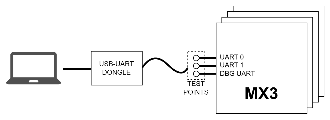
Figure 16 - UART Interface Connection
10. Thermal#
This section shows the thermal solution using on the M.2 Module for heat dissipation. The 4 cases below are the representative conditions to showcase the capability of the M.2 Module and thermal solution.
Cases |
1 |
2 |
3 |
4 |
|---|---|---|---|---|
Condition |
Worst |
Normal |
Low Power |
Low Power |
System TDP |
9.27W |
7.7W |
7.7W |
5.15W |
Ambient Temp |
70°C |
70°C |
50°C |
25°C |
Heatsink |
Yes |
Yes |
Yes |
No |
Airflow Requirement (Min) |
3 CFM |
2 CFM |
1 CFM |
1 CFM |
Table 6. Thermal Simulation Table
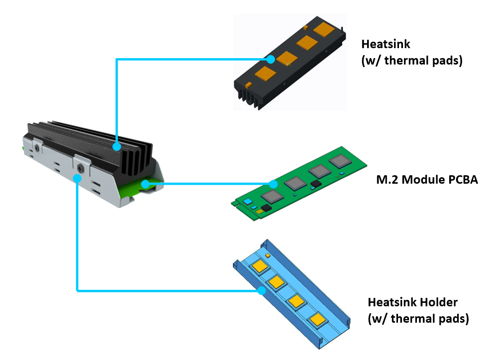
Figure 17 - Thermal Solution Assembly
Hint
If you’re designing your own PCBs using MX3 chips, please reach out to MemryX support so we can help guide you.
11. Use Cases#
This section demonstrates several use cases of the M.2 Module.
11.1 M.2 socket on Motherboard#
The user can insert the M.2 Module into any motherboard that supports a M.2 2280 M-key socket.
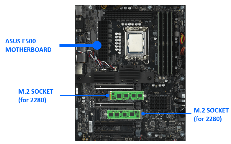
Figure 18 - M.2 Module On Motherboard
11.2 PCIe-M.2 adaptor on Motherboard standard PCIe slot#
User can insert the M.2 Module into the PCIe adaptor and install it into the standard PCIe slot on the Motherboard if there’s no M.2 socket.
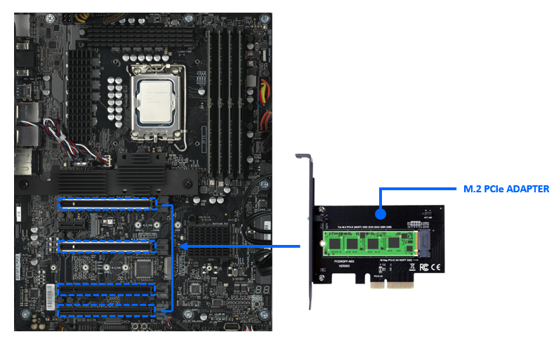
Figure 19 - M.2 Module On PCIe Adaptor
11.3 M.2 socket on embedded systems#
Orange Pi 5 is a small embedded system with one M-key M.2 socket, which is a good development platform. User can find a similar embedded system for their own development.
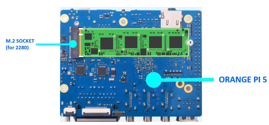
Figure 20 - M.2 Module On Embedded System
12. Disclaimer and Notices#
12.1 Copyright#
Copyright © 2024 MemryX Inc.
Published under the Creative Commons No-Derivates (CC-BY-ND) license.
12.2 General Notices#
To the fullest extent permitted by law, MemryX provides this document “as is” and disclaims all warranties, either express or implied, statutory, or otherwise, including but not limited to the warranties of merchantability, non-infringement of third-party rights, and fitness for particular purposes.
This document may inadvertently contain technical inaccuracies or other errors. MemryX assumes no liability for any such errors and for damages, whether direct, indirect, incidental, consequential, or otherwise, that may result from such errors, including but not limited to loss of data or profits.
The content in this document is subject to change without notice. MemryX reserves the right to make changes to document content without notification to users.

